Roll over image to zoom in
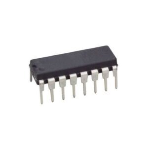
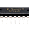
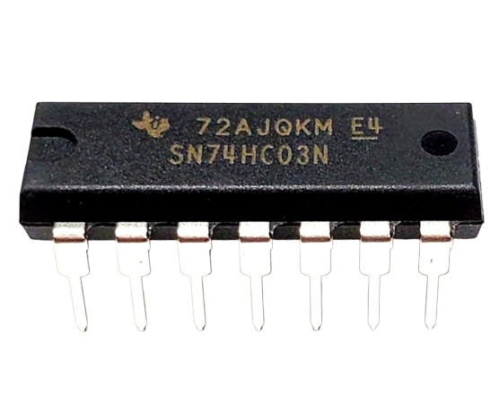
SN74HC03N DIP Quad 2-Input NAND Gate With Open Drain Outputs 7403
EGP25.00
Description
DIP Quad 2-Input NAND Gate With Open Drain Outputs 7403
This device contains four independent 2-input NAND gates. A key feature of this chip is its open-drain outputs , which allows the output to sink current to ground but not source current. This makes it highly versatile for applications like level shifting or creating wired-AND logic.
Features
- Wide Operating Voltage Range: 2 V to 6 V
- Open-Drain Outputs: Allows for flexible use in mixed-voltage systems and wired-AND configurations.
- Low Power Consumption: 20-μΑ maximum ICC
- Good Performance: Typical tpd = 8 ns at 5 V
- Low Input Current: 1 µA maximum
- Drive Capability:
- Outputs can drive up to 10 LSTTL loads
- ±4-mA output drive at 5 V
Specifications
| Specification | Detail |
|---|---|
| Logic Function | Quadruple 2-Input NAND Gate |
| Output Type | Open-Drain |
| Package | 14-pin PDIP (N) |
| Package Body Size (Nominal) | 19.30 mm × 6.40 mm |
| Parameter | Value |
|---|---|
| Supply Voltage (VCC) | 2 V to 6 V |
| Operating Free-Air Temperature (TA) | -40°C to 85°C |
| Input Voltage (VI) | 0 V to VCC |
| Output Voltage (VO) | 0 V to VCC |
| Parameter | Condition | Max Value |
|---|---|---|
| Supply Current (ICC) | VCC = 6V | 20 µA |
| Input Leakage Current (II) | ±1 µA | |
| Low-Level Output Voltage (VOL) | VCC = 4.5V, IOL = 4mA | 0.33 V |
| High-Level Output Leakage Current (IOH) | VO = VCC = 6V | 5 µA |
| Parameter | Condition | Max Value |
|---|---|---|
| Propagation Delay (Low-to-High) (tplh) | VCC = 4.5V | 31 ns |
| Propagation Delay (High-to-Low) (tphl) | VCC = 4.5V | 25 ns |

Applications
- LED Control
- Wired-AND Logic
- Voltage-Level Translation
- General Purpose Logic